Project summary
Scanning proximity probes (SPP) are uniquely powerful tools for molecular analyses and sensing; they are capable of addressing and manipulating surfaces at the atomic level and therein are keys to unlocking the full potential of nanotechnology. Current SPP nanotools are limited to several probes with optical readout and slow processing rates, mostly at the research level. This presently constitutes a severe limitation in the commercial/ manufacturing viability of this technology. Through the realization of modular parallel probe arrays with integrated piezoresistive readout and their individual and/or modular nanofunctionalisation, an avalanche of new tools and processes for a wide range of applications including sensing, electronics and the life-sciences industries would be viable. |
|
In this long-term research oriented project we expect to lead to a breakthrough in a new generation of tools for molecular level characterization and manipulation methods along the following directions:
A generic nanotool platform provided by a Parallel Modules of Nano-Electro Mechanical System (PM-NEMS) chip incorporating array of intelligent proximal probes with integrated actuator and piezoresistive readout, fully addressable, for high-speed data analysis or bottom-up product synthesis,
The modular generic NEMS-chip will be nanofunctionalised to generate a family of Application Specific NEMS-chip packages (AS NEMS) for integration into a range of new intelligent, cantilever based nanotools,
Prototypes of experimental nanotools based on the functionalised AS NEMS chips developed in TASNANO project will be produced and demonstrated in selected applications and the results used to support of the development of new nanotechnology processes and products.
It is the aim of TASNANO that the new modularly functionalised nanotools with PM ASNEMS chips inside' should empower nanotechnologists and drive the rapid development of nano-scale science, leading to new nanotechnology processes and, significantly, their industrial exploitation.
Development of handling and control devices and instruments for characterization and/or manipulation at molecular and atomic levels. The selected topic encompasses what we have described in the proposal as the top-down and bottom-up approaches to nanotechnology processes and products. The key to this classification lies in the functionalisation of the generic PM SPP chip to meet the requirements of a particular nanotechnology process.
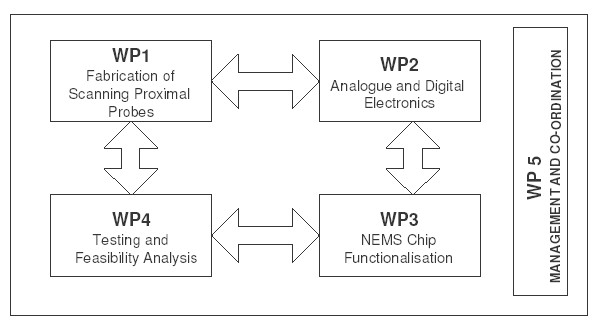
To achieve the technical goals of TASNANO project will require the integration of a range of scientific skills and facilities, including micro- and nanosystems technology, chemistry, surface science, biology, electronics, data processing and systems engineering. Teams from industry, academia and national research institutes will be drawn together in the STREP project. This is unique and exceptional opportunity to work together and develop new generation nanotools for characterization and manipulation at molecular level. The planned work will comprise of four science and technology Work Packages, each with dedicated objectives all working in a complementary manner. They are: (i) fabrication of massively parallel NEMS with integrated piezoresistive readout, (ii) analog and digital data path electronics, nano-position stage and experimental micro-chamber, (iii) NEMS chip, cantilevers and/or tips functionalisation, (iv) testing and demonstration. Management and Coordination will be a parallel activity running alongside all the work packages.
The most important output from TASNANO will be a prototype of instrument with several differently functionalised PM-SPP chips with measurement chambers, which together will provide multifunctional nanotools. Every change of the AS NEMS chip will create new application specific multifunctional instrument. In TASNANO the following application specific multifunctional nanotools will be developed:
- Multifunctional tool for manipulation - processes at molecular level,
- Tool for cell characterization and manipulation at molecular functional group level,
- Tool for label-free molecular characterization of chemical and biological activities,
- Multifunctional tool for thermal and electrochemical characterization,
- Tool for nano-patterning below 10 nm.
Micro-nano-engineering at the forefront of the field will be required, with radical new developments of cantilever microsystems into the NEMS regime. The nanoprobes themselves will be mechanically, physically, chemically or biologically customised for specific applications at high spatial resolutions. Our proposed nanotools will be useful for the fabrication of array of molecular switches, quantum computers, nano-patterning, bio- and environmental sensors, low-cost high resolution soft nanolithography molecular recognition, and in long-term a host of avalanche of other nanotool applications in the areas of engineering, biology, health care, communication industry etc. The diverse range of products is expected to create market opportunities within and outside the Community. Nanoscience and nanotechnology will be greatly advanced with the availability of the proposed nanotools.